|
Product Updates
Related Links
►
FPGA Boards
►
FMC Modules
►
SMT Manufacturing
|
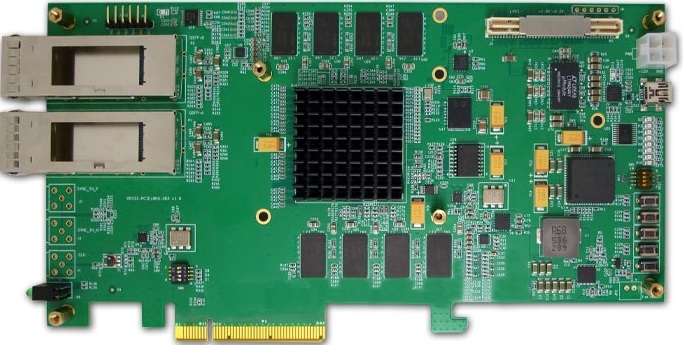
PCIe transceiver card based on VU9P 2CH 4 Gsps AD and 2CH 5Gsps DA
1. Overview
5Gsps AD DA transceiver PCIe board based on XCVU9P. The board is required to comply with the PCIe 3.0 standard, including a XCVU9P-2FLGA2014I, 2 groups of 64-bit/8GB DDR4, 2 high-speed AD, 2 high-speed DA, support external trigger, external clock. The operating temperature range of the board is 0 to 60°C. The design and processing of the board includes a heat sink, which supports air cooling and heat dissipation of the server. The software includes interface testing software, which supports Party A's application development. Second, the hardware composition  2.1 The logic hardware diagram of the board is shown in the figure:  2.2 Functional indicators Board function | parameter | content | A DC | Chip model | EV 10AQ190A | number of ways | 2-channel ADC, | Sampling Rate | 5G sps (actual work is 4Gsps) | data bits | 10bit _ | digital interface | DDRLVDS | analog interface | AC coupling | analog input | -250m V ~ 250m V | Connector | 2 -way SSMC (recommended model: S SMC - JYW HD ) | input resistance | 50Ω _ _ | Analog Indicator |
| DAC | Chip model | AD 9162 | number of ways | 2-way DAC | Sampling Rate | 5 G sps (actual work is 5 Gsps) | data bits | 1 6 bits | digital interface | JESD 204B _ | analog interface | AC coupling | Analog output | -200m V ~ 200m V _ _ _ _ | Connector | 2 -way SSMC (recommended model: S SMC - JYW HD ) | output impedance | 50Ω _ _ | Analog Indicator |
| clock 1 | PLL chip | AD 9516-1 | Onboard crystal oscillator | 1 0MHz temperature compensated crystal oscillator VCXO | External input clock | Default 10MHz , 3.3V LVTTL level, SSMC interface | clock 2 | PLL chip | HMC7044 | Onboard crystal oscillator | 100MHz VCXO | External input clock | SSMC interface | trigger | number of ways | 1 external input, SSMC interface. | level | 3.3V LVTTL level | FPGA | model | XCVU9P-2FLGA2014I | external cache | two groups of 64 -bit DDR4 onboard , each with a total capacity of 4 GB , and can work stably at 1200 MHz (2400MT/s) . | Loading method | piece of BPI Flash is used for program configuration, and one piece of SPI x4 NorFlash can be used for parameter storage . | PCIe | V3.0 PCIeX8 ; _ _ 2GB /s acquisition | digital interface | optical fiber | It supports 1 channel QSFP28 optical fiber interface, supports up to 4X 25 Gbps, and can be used for 100 G Ethernet development applications. | External IO | One single- ended to differential input, SSMC interface One differential to single- ended output, SSMC interface | GPIO | 14 GPIO backup use, four LED indicators , four user buttons . | software | operating system | Win 7 64 bit | Function | Triggered acquisition, continuous acquisition, hard disk storage, playback display | board standard | PCIe Specification | Board size | Full-height PCIe standard card | Board weight | (including heat sink) 1Kg | Board power supply | 12V(±10% ) ; 75W | Operating temperature | 0 to + 60 °C |
3 Software content Board hardware test; Flash loading test code; DDR4 test code, two groups work at the same time and work alone; AD, DA, clock configuration and acquisition interface program test (DA's Jesd204B IP uses Xilinx default version); PCIe3.0 x8 mode XDMA test, including FPGA code, driver under the PC of Linux system; Trigger signal test code; Other GPIO test code.
|
Accessories (FPGA Boards)
|
RSE-PCIE-04KU060:Xilinx Kintex® UltraScale™ PCI Express Development Platform
More info...
|
PCIe transceiver card based on VU9P 2CH 4 Gsps AD and 2CH 5Gsps DA
More info...
|

RSE-PCIE-04XC7V: Xilinx Virtex™ -7 PCI Express Development Platform
More info...
|
RSE-PCIE-04XC7K: Xilinx Virtex™ -7 PCI Express Development Platform
More info...
|
RSE-PCIE-02XC7K: Xilinx Virtex™ -7 PCI Express Development Platform
More info...
|
|
|